Hetero-junction (HJT) technology could be overlooked for several decades, but it has been taking momentum for the last years. 2023-2024. This shows its true potential to solve some common limiting factors for standard photovoltaic (PV) modules. It may help in reducing the recombination process and improving performance in hot climates.
If you want to learn the detailed description of HJT technology, this brief article will better help you. Here you will learn about the design and operability of an HJT cell, its difference when compared with other technologies, applications, benefits and many more.
What is a HJT solar panel?
HJT solar panels are specially designed similarly to the standard Homo-junction modules, but the specialty of this technology lies in the solar cells itself. The technology is engineered to fulfill the needs of the current demands and to fill the gap created by Longi Himo 6 and Jjinko N Type. To understand the unique technology of HJT, we provide you with a deep analysis of the materials, manufacturing, structure and classification of the HJT panels.
Materials required for manufacturing the Hetero-Junction Solar Cell:
There are most important materials required for making HJT cells:
- Indium Tin Oxide (ITO)
- Crystalline Silicon (c-Si)
- Amorphous Silicon (a-Si)
Crystalline Silicon is the basic material that is regularly used to create the standard Homo-junction solar cells, seen in conventional panels. There are two varieties of c-Si, Mono-crystalline and poly-crystalline Silicon. Mono-crystalline Silicon is the only standard element considered for HJT solar cells as it has a higher purity and best efficiency.
Amorphous Silicon is used in thin-film PV Technology and is the second most important material for manufacturing Hetero-junction solar cells. While a-Si itself has the density defects, applying a hydro-generating process solves them. It creates hydro-generated amorphous Silicon (a-Si-H) which is easier to dope and has a wider band-gap, making it better for creating HJT cells.
Indium Tin Oxide is also a preferred material used in HJT cells for the transparent conductive Oxide (TCO) layer of the Hetero-junction solar cell. But the researchers are investigating for using Indium-free materials that will reduce costs for this layer. The reflectivity and conductivity properties of ITO make it a better contact and external layer for the HJT solar cell.
Structure of the Hetero-junction Solar cells:
Standard Homo-junction solar cells are manufactured with c-Si for the N-type and P-type layers of the absorbing layer. Instead, HJT technology combines wafer-based PV technology (standard) with thin-film technology, providing Hetero-junction solar cells with their best features.

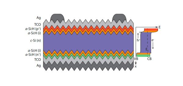
The absorber layer of the Hetero-junction solar cell is enclosed in a c-Si wafer-based layer (blue layer) placed between two thin intrinsic a-Si:H layers (orange layer), with a doped a-Si:H layer (red layer & Green Layer) placed on the top of each a-Si:H (i) layer. The number of TCO layers varies depending on the HJT cell being mono-facial or bi-facial. The rear layer is a metal layer which acts as the conductor for mono-facial Hetero-junction cells.
Manufacturing of HJT Solar Cell:
There are several steps that are involved in the manufacturing process of the Hetero-junction solar cell. The steps are as follow:
- Wafer processing.
- Wet-chemical Processing.
- Core-Layer deposition.
- TCO deposition.
- Metallization.
The wafer processing involves cutting the c-Si cells with a diamond based sharp saw. The process is performed with extreme delicacy which results in high-quality c-Si layers. It translates to a higher efficiency.
During the wet-chemical processing, Organic and metal impurities are removed from the c-Si wafer. Two methods are often used for wet-chemical processing: the RCA method, involving the use of concentrated sulfuric acid and hydrogen peroxide, and a cost-effective alternative applying an Ozone-based process.
After the wet-chemical processing, the deposition process is applied using Plasma-Enhanced Chemical Vaporization Deposition (PECVD). The process involves the depositing a-Si layers on both sides of the wafer-based layer.
The second part of the deposition process uses the physical Vapor Deposition (PVD) through sputtering to apply ITO, which forms the TCO layer of the Hetero-junction Solar cell. Another alternative process uses Reactive Plasma Deposition (RPD) to apply the TCO layer, but this is less popular option.
The metallization process is different from regular manufacturing process because the Hydrogen in a-Si:H limits the temperatures to a maximum of 200-220 ºC. A special type of curated Silver paste at low temperature is used through a Copper electroplating or screen printing process, to place the electrodes on the cell.
Classification of Hetero-junction Solar Cells:
Hetero-junction HJT solar cells are classified in two different categories depending on the doping: n-type and p-type.
The most popular doping uses n-typr c-Si wafers which are doped with Phosphorus. It provides them an extra electron to charge them negatively. These solar cells are resistant to Boron-Oxygen, which decreases the purity and efficiency of the cells.
The p-type solar cells are the best option for application for they are more resistant to radiation levels perceived in space. The p-type c-Si wafers are doped with Boron to provide the cells with one less electron which charge them positive.
How does HJT Solar Panel work?
Hetero-junction solar panels functions the same as other PV modules under the photovoltaic effect. The main difference of this technology lies in the fact that it uses three layers of absorbing materials combining thin film and traditional photo-voltaic technology. The process involves connecting the load to the terminals of the module, with the photons being converted into electricity. It may thus generate an electric current which flows through the load.
A photon impacts the P-N junction absorber and excites an electron, causing it to move to the conduction band and creates an electron-hole (e-h) pair and thus generates electricity.
The excited electron is collected by the terminal connected to the P-doped layer. This creates the flow of electric current through the load.
After the electricity flow through the load, the electron flows back to the rear contact of the cell and recombines with a hole. This constantly happens as the modules generate electricity.
A phenomenon, surface recombination, occurs in standard c-Si PV modules, which limits their efficiency. During this process, excited electron pairs at the surface of the material, causes them to recombine without the electron being collected and flows as an electric current.
To reduce the surface recombination, HJT cells separate the highly re-combinative (ohmic) contacts from the wafer-based layer using a passivating semi-conductor film with a wider band-gap layer made from a-Si:H. This buffer layer makes the charge trickle slow enough to create a high voltage. The high voltage is fast enough to avoid recombination before electrons are collected. It increases the efficiency for the HJT cell.
During the light-absorbing process, all of the three semi-conductor layers will be absorbing photons and converting them into electricity.
The first photons will be absorbed by the exterior a-Si:h layer, converting them into electricity. The majority of the photons are converted by the c-Si layer, the highest solar conversion efficiency among the materials in the cell. The remaining photons are finally converted by a-Si:H layer at the rear side of the module. This three-step process is the reason behind the mono-facial HJT solar cells’ the highest efficiency up to 26.8%.
Hetero-junction vs. Traditional Crystalline Silicon Panels:
HJT technology is based on the traditional c-Si panels, improving the recombination process and other major flaws. In this section, a brief comparison of how both the technologies differ may help us to understand a few modifications in the structure of the cell impact the overall performance of the module.
The HJT solar panel improves the deficiencies found in the standard c-Si modules, reducing surface recombination. This technology holds a higher recorded efficiency and improves the lifespan of the modules. Consequently, HJT panels have a lower temperature co-efficient, resulting in better performance under different extreme temperatures.
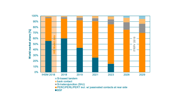
HJT technology was te first developed technology on the 1990s. it became popular in this last decade, which explains the 5% market share and higher production costs. But this is only a temporary setback that is expected to be surpassed in the near future.
Hetero-junction vs. Bifacial Panels:
The structure of Bifacial Panels is similar to the Hetero-junction Solar Panels. Both the panels include passivating coats which reduce the resurface combination. This coating increases its efficiency and endurance.
HJT technology maintains its high recorded efficiency of 26.8%, whereas the Bifacial surpasses it efficiency up to 30%. The curious side is that the Bifacial PV module used to achieve the efficiency combines HJT technology with Bifacial and other technologies.
HJT cell is also designed for Mono-facial or Bifacial usage. It reduces the reasons to compare them with each other. They can also be combined to create superior Bifacial HJT solar panels. The major difference lies in the fact that bifacial can use other base technologies that is different from HJT technology.
Benefits of Hetero-junction HJT panels:
HJT solar panels are highly beneficial since they have an improved technology with great potential in the solar industry. Major benefits of HJT technology are as under.
High Efficiency:
The high efficiency of 26.06% for Mono-facial modules and more than 29% for bifacial HJT places itself as one of the most efficient solar technology in the solar industry. This unique efficiency makes it convenient for applications with limited spaces like areas which require large generation capacities and others.
Good Temperature Co-efficient:
HJT solar cell technology is least affected by changes in temperature. It is the best option for applicants with high temperatures. Usually, high temperature can negatively affect the performance of standard c-Si modules but the case with HJT is quite different and efficient.
High Bi-faciality:
HJT cell technology has a very high Bi-facial factor of 92%. This specialty delivers a great performance when designed as a Bi-facial module. This technology has become more popular for utility-scale applications, which seek to take advantage of the Albedo resources.
Easy Manufacturing Process:
HJT solar cells have an additional step in the process of its manufacturing. This highly engineered structure does not affect its prices. This technology only involves 5-7 steps during manufacturing, and the prices for the necessary equipment are constantly being reduced. It shows a great promise for the future of HJT.
Application of Hetero-junction Solar Technology:
HJT solar panels are versatile to extreme level. It opens the ways for solar industry to further increase the applications for solar power. The following are some of the most common applications for this technology.
Limited Space Applications (Solar shingles and BIPV)
HJT’s high conversion efficiency makes it the greatest for limited space application. Two popular applications are manufacturing of Solar shingles and Building Integrated Photo-voltaic (BIPV) products. Tesla roofs are among the most popular shingles using this technology, which greatly increases its solar efficiency for home with photo-voltaic.
Power Source for Wearable Devices:
Its reduced size of wafer-based layers can open the way for integrating HJT technology with wearable devices. This provides the HJT devices with a powerful source to extend its autonomy during the days.
Utility Applications:
Regular mono-facial HJT solar panels may be used in utility-scale applications. It is beneficial with in solar farms with an average efficiency of over 30%. It does not only take advantage of direct sun but also from the Albedo resource. It is equally applicable in homes and commerce.
Future of Hetero-junction Technology:
The HJT technology is a promising technology with a highly recorded efficiency. This technology has made the ways for solar industry to increase the efficiency of the day-to-day PV module and decrease the leveled cost of energy (LCOE) regarding solar power.
The solar industry recorded 5GW in HJT solar panels in 2020, which makes it the highly retailed 5% market. It is the largest manufacturing panels, Tesla in USA and Panasonic in Malaysia and Japan. The future expectation is even brighter with an expected prices of 0.19$/W for 2030. It could hold 15-20% of the retail market in future.

On of major limiting factor for HJT is the current rate and process of manufacturing of the materials. With the developing technologies and comparison with other materials, the HJT is a promised quality which could increase efficiency and reduce costs for Hetero-junction solar panels.


